With the popularity of smartphones and the Internet of Things, the issue of chip power consumption has received more and more attention in recent years. In order to achieve the low power design goals of integrated circuits, we need to adopt a low power design solution at the system design stage. Moreover, with the gradual advancement of the design process, to the chip back-end design stage, there are few ways to reduce the power consumption of the chip, and the percentage of power consumption saved is also decreasing.
The power consumption of the chip is mainly composed of static leakage power and dynamic power. The static power consumption mainly refers to the power consumption caused by the leakage current when the circuit is in the waiting or inactive state, mainly including the reverse bias diode leakage current, the gate gate induced drain leakage current, the subthreshold leakage current and the gate leakage current. Dynamic power consumption refers to the power consumption caused by the transistor in the transition state. It is mainly composed of dynamic switching power consumption caused by dynamic switching current and short-circuit power consumption caused by short-circuit current. These concepts go to the reference book by yourself, and they are not detailed.
Then let's learn, in the digital back-end phase, what are the options to reduce the above power consumption.
The first solution is multi-supply multi-voltage technology, Multi supply Multi Voltage (MSMV). This is a technology that can effectively reduce dynamic power consumption. The chip can be divided into different voltage regions (Voltage Area), also known as Power Domain. Different logic modules are in different power domains and are powered by different power sources. The high-performance part is in the high-voltage domain, and the low-performance part is allocated in the low-voltage domain. For example, in a SOC chip, the CPU should work at the highest possible clock, then its voltage should be the highest voltage; and the USB module in the peripheral has a fixed rate defined by the protocol, as long as it is allocated to meet the requirements. The working voltage can be used; some modules that do not work normally can even turn off the voltage (Power Gating), which can make the power consumption tend to zero. Such a chip will be divided into various voltage domains.
So how do we create a Voltage Area?
First of all, we need to have a unified power constraint file, which is introduced with UPF. This file can be used in the whole chip development process from front-end gate-level netlist to final logic verification. There are not many orders, so it is eager to learn. In the next few articles, everyone and I worked with UPF files to learn about Low Power.
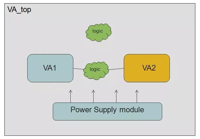
For example, we want to implement a simple MSMV design, VA1 and VA2 two different Voltage Area and defalut VA_top.

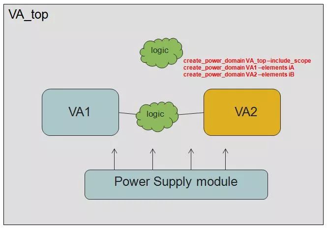
1. First define the information of the Voltage Area
Create_power_domain VA_top –include_scope default voltage area
Create_power_domain VA1 –elements iA VA1
Create_power_domain VA2 –elements iB VA2

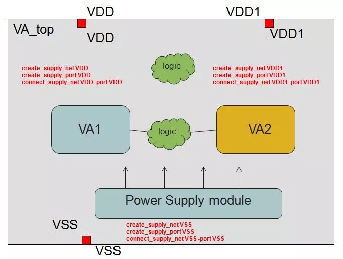
2. Create a power supply connection relationship on the default voltage area
Create_supply_net VDD creates supply net VDD
Create_supply_port VDD create supply port VDD
Connect_supply_net VDD -port VDD logically correlates VDD net and VDD port
Create_supply_net VDD1 create supply net VDD1
Create_supply_port VDD1 create supply port VDD1
Connect_supply_net VDD1 -port VDD1 logically correlates VDD1 net and VDD1 port
Create_supply_net VSS create supply net VSS
Create_supply_port VSS create supply port VSS
Connect_supply_net VSS -port VSS logically associates VSS net and VSS port

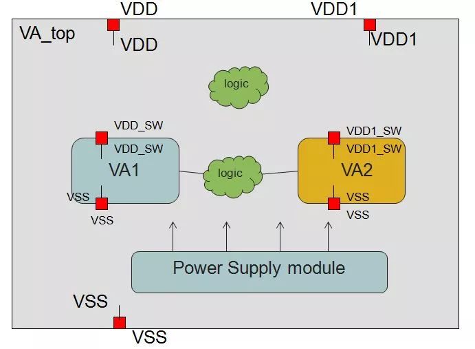
3. Create a power connection between VA1 and VA2 voltage area
Create_supply_port VDD_sw –domain VA1
Create_supply_port VDD1_sw –domain VA2
Create_supply_port VSS -reuse –domain VA2
Create_supply_port VSS -reuse –domain VA1
Create_supply_net VDD_sw –domain VA1
Create_supply_net VDD1_sw –domain VA2
Create_supply_net VSS -reuse –domain VA1
Create_supply_net VSS -reuse –domain VA2
Connect_supply_net VDD_sw –ports VDD_sw –domain VA1
Connect_supply_net VDD1_sw –ports VDD1_sw –domain VA2
Connect_supply_net VSS –ports VSS –domain VA1
Connect_supply_net VSS –ports VSS –domain VA2

4. Create a power collection, associated to the Voltage Area
Create_supply_set ss_top \ default voltage area set
-function {power VDD} \
-function {ground VSS}
Create_supply_set ss_pd1 \ VA1 set
-function {power VDD_sw} \
-function {ground VSS}
Create_supply_set ss_pd2 \ VA2 set
-function {power VDD1_sw} \
-function {ground VSS}
Associate_supply_set ss_top \
-handle VA_top.primary
Associate_supply_set ss_pd1 \
-handle VA1.primary
Associate_supply_set ss_pd2 \
-handle VA2.primary
Here, the definition of the voltage area in a UPF file is fine. After we read the UPF file and define the shape of the voltage area, we can see the voltage area on the GUI.
Aluminum Electrolytic Capacitors/ Ceramic Capacitors
Aluminum Electrolytic Capacitors/ Ceramic Capacitors
Aluminum Electrolytic Capacitors,Electrolytic capacitor,Ceramic Capacitor
YANGZHOU POSITIONING TECH CO., LTD. , https://www.pst-thyristor.com