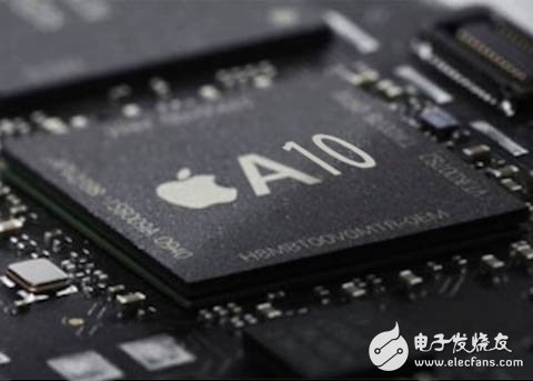
Apple will launch a new smart phone iPhone 7 (scratch) in the fall of 2016, which will be equipped with a fan-out wafer level package (Fan-out WLP; FOWLP) to make the new iPhone thinner and lighter. Lower.
So what is FOWLP packaging technology?
Fan Out WLP's English full name (Fan-Out Wafer Level Packaging; FOWLP), Chinese full name (fan-out wafer level package), which takes the way out of the cable, the cost is relatively cheap; fan out WLP can make a lot of different Bare crystal, the imaging WLP process is generally buried, equal to one layer of packaging, assuming that multiple bare crystals are placed, which is equivalent to saving multi-layer packaging, which helps to reduce customer costs. The only factor that affects IC cost at this time is the size of the die.
The Fan-out package was first proposed by Intel Mobil from 2009 to 2010 and is only used in mobile phone baseband chip packaging.
Since 2013, the world's major packaging and testing plants have actively expanded FOWLP production capacity, mainly to meet the demanding requirements of the low-cost smart phone market. Because FOWLP does not require the use of carrier materials, it can save nearly 30% of packaging costs, and the package thickness is also thinner, which helps to enhance the competitiveness of wafer vendors.

Advantage:
System in Package (SiP) combined with Embedded Printed Circuit Board (PCB) technology meets the needs of miniaturization of mobile devices, but there are problems with supply chain and cost. On the other hand, fanout The Fan-out Wafer Level Package (FoWLP) is not only less difficult to design than the Through Silicon Via (TSV) 3D IC, but also close to the 2.5D IC concept and relatively low cost, and is expected to become an advanced package. Key points of technology development.
challenge:
Although Fan-Out WLP can meet the demand for more I/O quantities. However, if you want to apply a lot of Fan-Out WLP technology, you must first overcome the following challenges:
(1) Thermomechanical behavior of solder joints: Since the structure of the Fan-Out WLP is similar to that of the BGA mount, the thermomechanical behavior of the Fan-Out WLP solder joint is the same as that of the BGA mount, and the key position of the solder ball in the Fan-Out WLP Below the silicon wafer area, the point of maximum thermal expansion coefficient mismatch occurs between the silicon wafer and the PCB.
(2) Accuracy of wafer position: When reconstituting the wafer, it is necessary to maintain the position of the wafer from the pick and place on the carrier without shifting, even during the molding operation. Offset. Because the dielectric layer is open, the redistribute layer (RDL) and the solder opening (Solder Opening) are all made using yellow lithography, the reticle is aligned with the wafer and the exposure is one-off, so the position of the wafer is accurate. The requirements are very high.
(3) Wafer warping behavior: Manually reconstructing the Warpage behavior of the wafer is also a major challenge because the reconstituted wafer contains plastic, silicon and metal materials, and the ratio of silicon to colloid is at X. The Y, Z and Z directions are different. The heat expansion and contraction of the mold during heating and cooling will affect the warpage behavior of the wafer.
(4) Peeling phenomenon of colloid: When water is absorbed by colloid and other polymers at normal pressure, when reflowing at 220~260°C, the water will vaporize instantaneously, resulting in high internal vapor. Pressure, if the composition of the gel is poor, it is easy to have colloidal peeling.
Impact on the PCB market:
At the beginning of this article, Apple will use this packaging technology on the iPhone 7 launched in the second half of this year. Since Apple can sell hundreds of millions of iPhones a year, if the FOWLP package is adopted in the future, it will inevitably affect the demand of the printed circuit board market.
In the printed circuit board market, printed circuit boards for semiconductors are among the more valuable products. In 2015, the global semiconductor printed circuit board market was about 8.4 billion US dollars, but in the face of new technology and Apple's decision-making impact, it is difficult to maintain the same market size in the future.
Therefore, the industry predicts that FOWLP technology may be extended to other parts in the future, and other industry players may follow up. Therefore, the shrinking of the printed circuit board market is only a matter of time.
Cylindrical Battery-Contacts And Clips
Cylindrical Battery Contacts Clips Springs
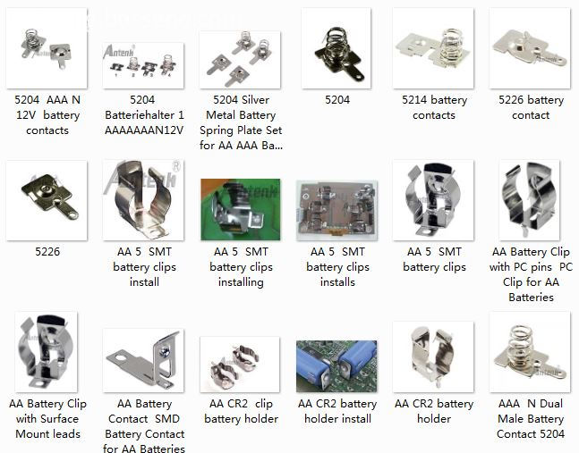
Antenk provides a wide variety of cylindrical battery contacts in various mounting styles
Antenk manufactures battery contacts, clips and springs for use with cases that have molded battery compartments, as well as for PCB mounting. These cost effective contacts allow a battery holder to be designed right into the body of the device while guaranteeing strong electrical connectivity with MPD's high quality battery contacts and springs. Antenk makes contacts and springs for use with all popular battery sizes, as well as some generic contacts for use with other types of cells.
Cylindrical Battery Contacts Clips Springs Features
Available in surface-mount, through-hole, and custom mounting options
RoHS 2 compliant
Used in conjunction with AAAA, AAA, AA, C, and D batteries

Battery Holder,Cylindrical Battery Contacts ,Cylindrical Clips,Cylindrical Contacts, Battery the Contacts,AAAA Contacts,AAA Contacts, AA Contacts, C Contacts
ShenZhen Antenk Electronics Co,Ltd , https://www.antenk.com