"The system is being updated, please do not turn off the power." We have seen this warning, which usually occurs when the electronics are to be updated in the flash installation code. If the update is interrupted, the flash will not be updated properly, the code will be corrupted, and the device will not run, ie "bricked". This well-known warning exists because most semiconductor devices that use flash memory need to be powered all the time during a program or erase operation. Obviously, it is very important to prevent the "brickming" of the device. But is it enough to just issue a warning? Some embedded devices do not even have a user display and therefore cannot generate a warning. How can we ensure reliable and secure remote system updates in our design?
The importance of remote upgrade of embedded systemsRemote upgrades are increasingly important for connected embedded systems. Remotely fixing vulnerabilities or adding new features over the Internet can save a lot of maintenance costs; when deploying thousands of embedded systems, maintenance is a big problem. As embedded systems security issues continue to increase, it is increasingly important to fix potential security vulnerabilities through remote security directed code upgrades. Obviously, the upgrade must be done securely, otherwise the attack algorithm can easily break the system with unsafe updates. Below is an example of a typical system that helps to better understand the requirements of a secure and reliable remote upgrade facility.
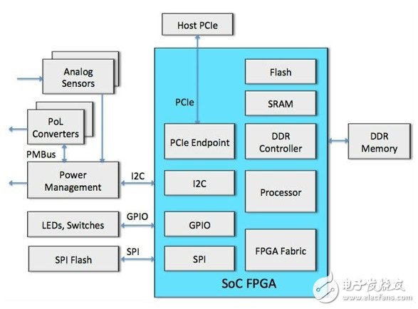
System example - control plane bridgeA Control Plane Bridge within a communication or network chassis is an example of a common system that requires remote updates. This subsystem brings together many low-speed peripherals such as analog sensors, power management modules, fans, fault logging memory, and status outputs using I2C, SPI, and GPIO interfaces. Then, you can use a faster bus—perhaps a PCIe, a common subsystem interface in communications and networking chassis—to communicate directly with low-speed peripherals. This chassis control subsystem is capable of implementing intelligent aggregation functions that "propel" communications when specified start-up points are activated, such as when reaching the highest or lowest voltage level. Figure 1 shows a system implemented with an FPGA (commonly referred to as a SoC FPGA) with an on-chip microcontroller.

Figure 1 Chassis Control Plane Bridge Upgraded Remotely via PCIe
FPGA and flashIn the above example, the remote update is implemented via the PCIe bus, but does not protect against power outages that may occur during programming. Let's take a look at the common types of FPGA implementations to better protect against major failures that can occur during sudden power outages during flash remote updates.
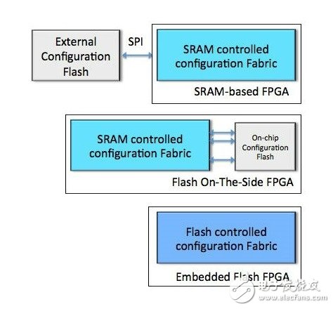
Almost every FPGA-based system requires some form of non-volatile memory to store configuration storage. In general, the configuration memory is located off-chip or on the chip. SRAM-based FPGAs require an external flash memory for configuration at power-up. Flash-based FPGAs can use configuration memory embedded in an FPGA fabric (structure embedded in a flash FPGA) or use an SRAM-based architecture, but place a flash block on the chip (side flash FPGA).
SRAM-based FPGAs typically use NOR SPI flash because they consume the fewest pin counts, and several vendors have the same pinout and density up to 1 Gb. Current NOR SPI flash devices have a 32-bit address selection that scales to 4GB devices without the need to change instruction and control protocols. What happens when this SPI flash is in program or erase mode (charge pump startup) and power is gone? Where does the charge disappear? Is there a circuit that detects the power failure of these flash memories and safely directs the charge to the ground? In general, data corruption occurs on pages that are being written.

Figure 2 Three FPGA configuration diagrams: SRAM-based FPGA with externally configured flash, side flash FPGA, and embedded flash FPGA
The side flash FPGA system uses a wider on-chip data bus to load SRAM-based configuration storage on power-up. Typically, this method loads the configuration faster than an SRAM-based FPGA because the latter uses external flash to configure the device. However, this approach has the problem of power loss during the program or erase cycle. Where did the charge go? Is the flash destroyed? Is the write-only page corrupted? Is there a risk in the entire flash memory? Is the FPGA capable of detecting corrupted on-chip memory, or is the corrupted data loaded into the configuration memory during power-up?
The destruction of flash memory is a problem, and how to ensure the security of remote data is also very important. When an embedded product is accessible by an end user, there is a possibility of being tampered with. In order to prevent attacks, both software and hardware security functions must be used. Encrypting only remote configuration data files is not enough. While this software encryption is safe and useful, the hardware (FPGA) that decrypts the data must also be placed in security. Encrypted data files are easily extracted when a user accesses an embedded device. This can be achieved with inexpensive electromagnetic probes and differential power analysis (DPA). There are many examples of using this method to extract FPGA security keys. If the FPGA does not have built-in DPA countermeasures, there is a security risk for any remote updates. When users can access embedded products, if there is no DPA countermeasures, it will be like a large door, there is no security.
In FPGAs embedded in flash, the configuration is stored on-chip and tightly integrated into the FPGA fabric. For example, on the Microsemitech SmartFusion2 and IGLOO2 flash FPGAs, programming via an external communication port such as USB, PCIe or JTAG, the entire programming process is managed by an on-chip dedicated programming interface. In addition, SmartFusion2 and IGLOO2 FPGAs use a high-level programming mechanism called Programming in the Application (IAP) that provides reliable and secure programming even with power loss during programming. Let's look at how to use the IAP mechanism to achieve the reliable remote upgrade capabilities that today's embedded systems require.
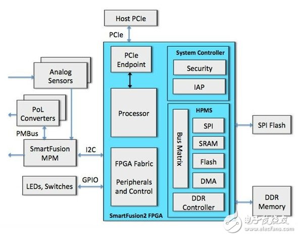
Reliable and secure remote updates in FPGA-based embedded systemsFPGAs embedded in flash can provide the key functions needed to easily support secure and reliable remote updates. For example, SmartFusion2 has all the major FPGA features needed to implement critical bridging and security and IAP capabilities. As shown in Figure 3, the low-speed interface can be connected by I2C and GPIO. The high-speed host interface PCIe acts as a dedicated port that does not require an FPGA fabric.

Figure 3 SmartFusion2 "In-Application Programming" (IAP) supports chassis control plane bridge for secure and reliable remote updates
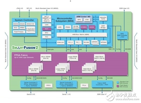
The on-chip processor can use the High-Speed ​​Memory Subsystem (HSMS) to access large internal flash memory for code storage, access large internal SRAM for data buffering, and dedicated DDR controllers to access other external memory when needed. The dedicated system controller provides the security features used during programming and the IAP functions used during remote updates. Figure 4 details the key features available on the SmartFusion2 FPGA.

Figure 4 Microsemi's SmartFusion2 SoC FPGAs have mainstream features and reliable security and remote update capabilities
Secure and reliable upgrades with "programming in the application"The IAP mechanism provided by SmartFusion2 and IGLOO2 is a secure and reliable way to remotely update the configuration bitstream. The IAP is executed by the dedicated system controller within the FPGA, so there is no need to use any FPGA fabric or other user configurable logic. The IAP function uses an external SPI flash device and is a two-step process. In the first step, the external SPI flash device is programmed with the required bitstream through any available interface, such as PCIe, USB, JTAG or even Ethernet. All bitstreams used for SmartFusion2 device programming are encrypted to ensure they are not tampered with.
In the second step, the system controller requests the execution of the IAP service through the system service. The user provides a pointer to the system controller that points to the initial address of the bitstream location within the external SPI flash. The IAP system service request also has three user options: authentication, programming, or verification. Authentication is typically performed prior to FPGA configuration memory programming to verify that the bitstream within the SPI flash is suitable for the device being programmed. The device is operating normally during authentication.
The external SPI flash containing the new bitstream also contains an additional image, a good version for recovery purposes. The user can configure the FPGA to a good state using the recovery image at any point in time. The recovery image can be saved "as is" or updated as needed for the repair of critical vulnerabilities.
Program recovery can be used during IAP function implementation. If power is lost during programming, program recovery is initiated and the system controller will disable the internal charge pump of the programming FPGA in a controlled manner. During the next power cycle, before starting the FPGA fabric, the system controller will detect that the device programming operation has been interrupted and it will initiate the programming cycle from the bitstream in the external SPI flash. Users can choose to update from a good image or from a remote update image that has just been pushed to the SPI flash. When the external bitstream is loaded into the SmartFusion2 FPGA, it uses built-in DPA countermeasure logic to ensure that no electromagnetic probe can decrypt the encryption key, providing a trusted security device for the embedded system.
Used in conjunction with secure encrypted bitstream and bitstream verification, program recovery provides a secure and reliable remote programming update mechanism for currently connected embedded systems, even if the FPGA configuration memory is interrupted during the programming process.
The 80mm ultra-large paper warehouse is embedded with a thermal printer and supports a variety of communication interfaces, such as RS232, TTL, USB and other communication interfaces, allowing more users to accept it and making the product more friendly. It is widely used in large-scale self-service terminal equipment such as medical treatment and factories. Its appearance design is simple and supports the development of various systems. It does not need carbon ink, adopts thermal printing technology, and only needs thermal paper roll to print all kinds of content. It is an economical and fast printing. Support the secondary development of major systems. There are two types of manual tearing and automatic cutting.
80Mm Embedded Label Printer,80Mm Large Paper Warehouse Printer,Embedded Thermal Label Printer,Printer Thermal 80Mm Auto Cutter
Shenzhen Geyi Technology Co., Ltd. , https://www.gy-printer.cn