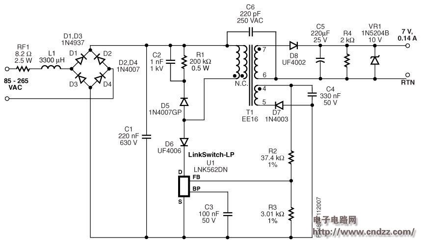
Summary:
Universal input with a LNK562DN design, 0.98 W output flyback power supply. The power supply output is 7 V, 0.14 A (1W) with loose constant voltage/constant current (CV/CC) characteristics. This power supply replaces two electrolytic capacitors in series with a low value metal film capacitor of 630 V rated voltage. This design is ideal for single-phase meters or applications that must withstand AC input voltages up to 350 VAC in a matter of minutes.
0.98W Flyback Power Supply Design Features
- No need to use input bulk capacitors
- Increased reliability of products used in areas with severe input voltage fluctuations
- Saves on the superposition of two electrolytic capacitors for increasing the voltage rating
- PCB space and reduced costs
- Extremely energy efficient
- Meets CEC/Energy Star 2008 requirements for work mode efficiency (required
- 50%, up to 55%)
- Low input power at no load (no-load power consumption is less than 230 VAC AC input)
- 200 mW, required to be 500 mW)
- Low cost, low component count, alternative to compact and lightweight linear power supplies
- No optocoupler required
- No constant current detection resistor required
- Simple EMI filter in accordance with EN55022B
Circuit diagram of 0.98W output flyback power supply

See the uploading documentation for details (click to download)
Dongguan Pinji Electronic Technology Limited , https://www.iquaxusb4cable.com