The most troublesome part of designing a switch mode power supply is the RCD buffer. The conventional method of designing an RCD buffer has no detailed description of the off-state transients of the main switch. Therefore, the design equations in the traditional design are not completely correct. This article describes a new approach to designing and analyzing RCD buffers for flyback converters. The resonant coordinates provide an easy way to understand the main switch off transients and help to easily design and analyze the RCD buffer.
1 Introduction
Commercially, flyback converters are widely used due to their simple construction, compact size, light weight, and low cost. However, its main switch performs a hard switching operation, resulting in higher voltage spikes and oscillations on the main switch. The voltage stress of the main switch increases depending on the magnitude of the voltage spike. To reduce voltage spikes in order to use lower cost, low voltage MOSFETs, the most widely used method is the RCD buffer network. Even if the buffer voltage decreases as the snubber resistance decreases, the power consumption on the buffer network increases, resulting in a decrease in overall system efficiency. Therefore, the RCD snubber network should be optimized to meet both the main switching voltage stress and the overall system efficiency.
This article will first introduce the traditional analysis of voltage spikes caused by the leakage inductance of the main transformer. A simple way of describing the off transient period will be introduced for further analysis. The buffer current will be analyzed in the buffer coordinates to provide a more detailed design equation.
2. RCD buffer design and analysis
2.1 General method of RCD buffer design
Figure 1 shows a conventional flyback converter with an RCD buffer.
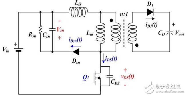
Figure 1: Traditional Flyback Converter
The RCD snubber circuit is used to clamp the voltage spike caused by the resonance between the leakage inductance Llk and the main switch drain to the source capacitance CDS. There are a number of assumptions to describe how it works to design an RCD buffer, as follows:
(1) Vsn"nVout and Vsn are almost constant due to the large Csn:
(2) CDS=COSS+CTRANS, regardless of vDS(t):
(3) When the main switch Q1 is turned off, there is no secondary side leakage inductance, so iDS(t) can be instantaneously transmitted to the secondary side diode current iD1(t), where Csn is the snubber capacitor and CDS is the main switch drain and source The effective capacitance between the poles, COSS is the output capacitance of the MOSFET, CTRANS is the effective capacitance between the primary circuit terminals of the transformer, vDS(t) is the voltage between the main switches, and iDS(t) is the current flowing through the main switch. Q1 is the main switch.
Figure 2 shows the equivalent circuit when the snubber diode is conducting.
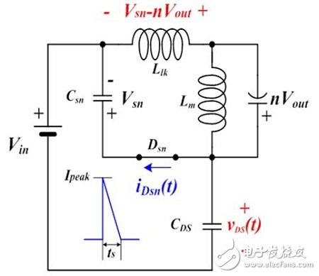
Figure 2: Equivalent circuit during the snubber diode turn-on
When switch Q1 is turned off, the main current charges the COSS of Q1 (while discharging the CTRANS of the transformer). When COSS is charged to Vin+nVout, the secondary side diode is turned on, energy is transferred to the secondary side, and COSS is continuously charged because the leakage inductance Llk still has some residual energy. When vDS(t) of Q1 is increased to Vin+Vsn, the snubber diode Dsn is turned on, and vDS(t) is clamped at Vin+Vsn. When Dsn conducts, the voltage on Llk is Vsn-nVout, so the turn-on time of Dsn(ts) can be obtained as follows:
 (1)
(1)
Where Ipeak is the peak drain current before the switch Q1 is turned off. There are two ways to calculate the power consumption (Psn) in the buffer network; the power supply through Dsn and the power consumption in Rsn are as follows:
 (2)
(2)
Where fsw is the switching frequency of the flyback converter. Therefore, the snubber resistance Rsn can be obtained by the following equation:
 (3)
(3)
This is the traditional way of looking up the snubber resistor Rsn. However, after several steps of LC resonance, the peak drain current Ipeak is reduced a little. Therefore, equation (3) may mislead an over-engineered system.
Let us use the resonant coordinates to get the actual peak drain current to avoid over-engineering the RCD buffer in the next section.
2.2 Design and Analysis of RCD Buffer in Resonant Coordinates
This section will design the RCD buffer using the resonant coordinates. When designing the buffer only, there is no need to analyze the entire flyback mode of operation. Figure 3 shows the equivalent circuit for each mode, and Figure 4 shows the vDS(t) of the switching MOSFET in the flyback converter.
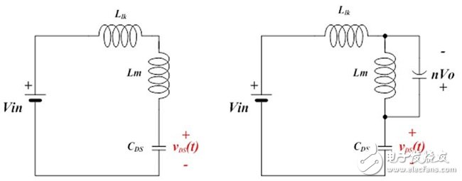
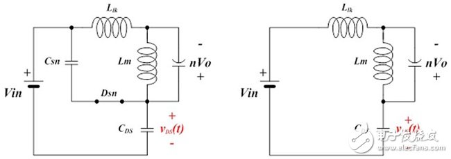
Figure 3: Equivalent circuit for each mode displayed after the main switch is turned off (modes 1 to 4 in order)
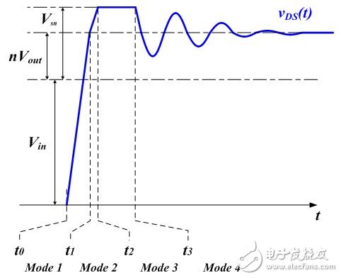
Figure 4: vDS(t) after the switch is turned off
An Audio Cable, referred to as an audio cable, is used to transmit electrical acoustic signals or data. Broadly speaking, there are two major categories of electrical signals and optical signals. The line that the audio cable uses to spread the sound. It consists of two parts: the audio cable and the connector. The audio cable is usually a two-core Shielded Cable. The common connectors are RCA (commonly known as lotus head), XLR (commonly known as card head), and TRS JACKS (commonly known as plug head).
Chinese name
Audio Lineeffect
Used to transmit electroacoustic signals or data
Generalized classification
Electrical and optical signals
composition
Audio cable and connector
Full name
Audio cable
connection method
Balanced connection, unbalanced connection
classification
Audio electric signal cable, audio optical signal cable
Audio Cable
Audio Cable,Optical Audio Cable,Digital Optical Audio Cable,Rca Audio Cable
Jiangsu QiSheng Cable Co., Ltd. , https://www.shuaihe-cable.com