Circuit function and advantage
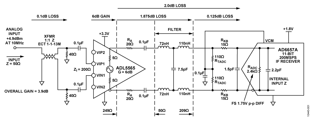
The circuit shown in Figure 1 is based on the ultra-high dynamic range differential amplifier driver ADL5565 and the 65 MHz bandwidth receiver front end of the 11-bit, 200 MSPS quad IF receiver AD6657A.
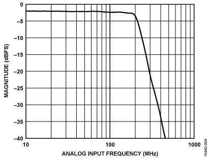
The fourth-order Butterworth anti-aliasing filter is optimized based on the performance and interface requirements of the amplifier and IF receiver. The total insertion loss due to the filter network and other resistive components is only 2.0 dB. The overall circuit bandwidth is 65 MHz, the low-pass filter has a 1 dB bandwidth at 190 MHz and a 3 dB bandwidth at 210 MHz. Passband flatness is 1dB.
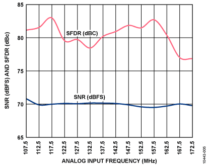
The circuit is optimized for processing a 65 MHz bandwidth IF signal centered at 140 MHz and sampling at 184.32 MSPS. The SNR and SFDR measured with a 140 MHz analog input in the 65 MHz band are 70.1 dBFS and 80.9 dBc, respectively.

Figure 1: Single channel at the front end of a four-channel IF receiver (schematic diagram: all connections and decoupling not shown) Gain, loss, and signal level measured at 10 MHz
Circuit description
The circuit shown in Figure 1 accepts a single-ended input and converts it to a differential signal using a wide bandwidth (3 GHz) M/A-COM ECT1-1-13M 1:1 transformer. The ADL5565 6.0 GHz differential amplifier operates with a differential input impedance of 200 Ω with 6 dB gain, 100 Ω with 12 dB gain operation, and 67 Ω with 15.5 dB gain operation.
The ADL5565 is the ideal driver for the AD6657A, which provides a fully differential architecture in the ADC through a low-pass filter, providing good high-frequency common-mode rejection while minimizing second-order distortion products. The ADL5565 provides 6 dB, 12 dB, and 15.5 dB gain based on the input connections. In this circuit, the insertion loss of the 6 dB gain compensation filter network and the transformer (approximately 2.1 dB) is used to provide a total signal gain of 4.0 dB. The gain also helps to minimize the noise effects of the amplifier.
The AD6657A is a four-channel IF receiver that internally connects each ADC output to a digital noise shaping requantizer (NSR) module. The integrated NSR circuit improves the signal-to-noise ratio (SNR) performance of the smaller bands within the Nyquist bandwidth.
The NSR module can be programmed to provide a bandwidth of 22%, 33%, or 36% of the sample rate. For the data used in this circuit note, the sampling rate is 184.32 MSPS and the following NSR settings apply:
NSR bandwidth = 36%
Tuning word (TW) = 12
Left band edge = 11.06 MHz (input = 173.26 MHz)
Center frequency = 44.24 MHz (input = 140.08 MHz)
Right band edge = 77.41 MHz (input = 106.91 MHz)
For details on how to work with the NSR module, see the AD6657A data sheet.
The anti-aliasing filter is a fourth-order Butterworth low-pass filter designed using a standard filter design program (in this case, Agilent ADS). The Butterworth filter was chosen because of its flat response. The fourth-order filter produces an AC noise-to-noise ratio of 1.03. Other filter design procedures are available from Nuhertz Technologies (http://) or Quite Universal Circuit Simulator (Qucs) Simulation (http://).
For best performance, the ADL5565 should load a net differential load of at least 200 Ω. A 20 Ω series resistor isolates the filter capacitor from the amplifier output and produces a net load impedance of 249 Ω when added to the downstream impedance.
A 15 Ω resistor in series with the ADC input isolates the internal switching transients from the filter and amplifier. A 110 Ω resistor in parallel with the ADC is used to reduce the input impedance of the ADC, making performance more predictable.
The differential input impedance of the AD6657A is in parallel with 2.2 pF and is approximately 2.4 kΩ. For this type of switched-capacitor input ADC, the real and imaginary parts are a function of the input frequency; for a detailed analysis, see the application note AN-742.
The fourth-order Butterworth filter is designed with a source impedance of 50 Ω, a load impedance of 209 Ω, and a 3 dB bandwidth of 190 MHz. The final circuit value of the filter is shown in Figure 1. The values ​​generated from the filter program are shown in Figure 2. The value chosen for the filter passive component is the standard value closest to the program generated value. The ADC's internal 2.2 pF capacitor is used as the final shunt capacitor for the filter design.
As can be seen from this design, the best performance can sometimes be an iterative process. The filter programming value is very close to the final value, but the final value of the filter is slightly different due to some board parasitic capacitance. Figure 3 shows the final design values ​​of the filter.

Figure 2. Initial design of the filter program for a fourth-order differential Butterworth filter, ZS = 50 Ω, ZL = 209 Ω, FC = 190

Figure 3. Final design value of a fourth-order differential Butterworth filter, ZS = 50 Ω, ZL = 209 Ω, FC = 190 MHz
Table 1 summarizes the measurement performance of the system with a 3 dB bandwidth of 210 MHz. The total insertion loss of the network is approximately 2 dB. Figure 4 shows the bandwidth response of the final filter circuit, and Figure 5 shows the SNR and SFDR performance.
Table 1. Measurement performance of the circuit


Figure 4. Passband flatness performance versus input frequency

Figure 5. SNR/SFDR performance versus input frequency
SC/APC Fiber Optic Fast Connector
Sc/Apc Fiber Optic Fast Connector,Fiber Optic Adaptor Fast Connector,Fiber Quick Connect Kit,Sc Fiber Optic Fast Connector
Ningbo Fengwei Communication Technology Co., Ltd , https://www.fengweicommunication.com