Author: Cathal Murphy / Yao Fu
In order to meet the ever-increasing demand for data processing, future systems need to be improved in computing power. Traditional solutions (such as x86 processors) can no longer provide the required computing bandwidth in an efficient, low-cost manner, so system designers must find new computing platforms.
More and more system designers see Field Programmable Gate Arrays (FPGAs) and graphics processors (GPUs) as computing platforms that can meet future needs. This article will analyze the future GPU, FPGA, and system-on-chip (SoC) components to provide the necessary computing efficiency and flexibility for the new era.
Future systems such as cloud data centers and self-driving cars need to be improved in computational capabilities to support increasing workloads and evolving underlying algorithms [1]. For example, sensor fusion workloads for big data analytics, machine learning, vision processing, genetics, and advanced driver assistance systems (ADAS) exceed the efficiency and cost-effectiveness that existing systems (such as x86 systems) can provide.
System architects are looking for a new computing platform that meets their needs, and the platform needs to be resilient enough to integrate into existing architectures and support various workloads and evolving algorithms. In addition, many of these systems also need to provide deterministic, low-latency performance to support the fast response times needed for real-time systems such as self-driving cars.
Due to the achievements of GPUs in the field of machine learning training in the field of high performance computing (HPC), GPU vendors are very active in positioning the GPU as the best choice for a new era of computing platforms. In the process, GPU vendors have modified their architecture to meet the workload of machine learning inference.
However, GPU vendors have been ignoring the limitations of the GPU's basic architecture. These limitations can seriously affect the ability of the GPU to provide the necessary system-level computing performance in an efficient and cost-effective manner. For example, in a cloud data center system, the workload requirements will change greatly within a day, and these workloads The underlying algorithm is also rapidly evolving. The limitations of the GPU architecture can prevent many current and future workload images from being mapped to the GPU, resulting in idle or inefficient hardware. The chapters mentioned later in this article will introduce more detailed descriptions of these limitations.
Conversely, FPGAs and SoCs have many important qualities that will be the best choice for future system requirements. These unique qualities include:
・ Provides high computing power and efficiency for all data types
・ Provides high flexibility for multiple workloads and maximizes the benefits of computing and efficiency
・I/O flexibility, easy integration into the system and higher efficiency
・ Large chip built-in cache to provide high efficiency and lowest delay rate
See the background / application / advantages and disadvantages of the graphics processor large dismantlingThe origin of GPUs dates back to the PC era, and NVIDIA claims to have introduced the world's first GPU in 1999, but in fact many graphics cards were launched earlier [2]. The GPU is a newly designed product for sharing and speeding up image processing tasks, such as masking and converting pixel arrays from the CPU, making its architecture suitable for high parallel transfer rate processing [3]. In essence, the main role of the GPU is to provide high-quality images for visual displays (VDUs).
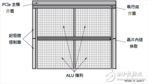
Figure 1 GPU module diagram
Over the years, such as the medical imaging applications of large-scale matrix operations, such a small number of non-imaging but massively parallel and memory-relevant workloads have been implemented from the GPU rather than the CPU. GPU vendors are aware that there is an opportunity to expand the GPU market to non-imaging applications, so GPU non-image programming languages ​​like OpenCL emerge as the times require, and these programming languages ​​translate GPUs into general-purpose GPUs (GPGPUs).
・Machine learningRecently, one of the workloads that can be well mapped to the GPU runtime is machine learning training. By fully utilizing the GPU, the training time of deep neural networks can be significantly shortened.
GPU vendors are trying to use the success of machine learning training to influence their development in machine learning inference (deploying trained neural networks). With the evolution of machine learning algorithms and the required data accuracy, GPU vendors have been adjusting their architecture to maintain their position. One example is that NVIDIA supports INT8 in its Tesla P4 product, but many users today are exploring lower precision such as binary and ternary [4]. To take advantage of machine learning and other areas of development, GPU users must wait for new hardware to be available before they are purchased.
GPU vendors want to use machine learning as their basis to make themselves the preferred computing platform for this new computing era. However, if we want to clearly understand whether the GPU is suitable for future systems, we still need to do a more comprehensive system-level analysis, consider the limitations of the GPU architecture, and how the system will evolve over time.
・ GPU architecture limitationsThis section will delve into the typical GPU architecture to expose its limitations and how to apply it to various algorithms and workloads.
・SIMT ALU arrayFigure 1 shows a typical GPU module diagram. At the heart of general-purpose GPU computing functions are large arithmetic logic units (ALUs) or computational cores. These ALUs are generally considered single instruction multiple threads (SIMT), similar to single instruction multiple data (SIMD).
The basic principle is to divide the workload into thousands of parallel threads (Threads), and the ALU needs a large number of GPU threads to prevent idleness. After the threads are scheduled, different ALU groups can execute the same (single) instruction in parallel. By using SIMT, GPU vendors can provide smaller and more efficient solutions than CPUs because many core resources can be shared with other cores in the same group.
However, it is clear that a particular workload (or part of the workload) can be effectively mapped to this massively parallel architecture [5]. If the threads that make up the workload do not have enough commonality or parallelism, such as continuous or moderately parallel workloads, the ALU will appear to be idle, resulting in reduced operational efficiency. In addition, the threads that make up the workload are expected to maximize ALU utilization and create delays. Even with independent thread scheduling in NVIDIA's Volta architecture, the underlying architecture still maintains SIMT as if massive parallel workloads are required.
For continuous, moderately parallel, or sparse workloads, the GPU provides less computational and efficiency than the CPU can provide [6]. One of the quantification examples is to perform sparse matrix operations on the GPU; if the number of non-zero elements is small, and from the perspective of performance and efficiency, the GPU is lower or equal to the CPU [7][8]. Interestingly, many researchers are studying sparsely convoluted neural networks to exploit large-scale redundancy in convolutional neural networks [9]. This trend clearly represents the challenges GPUs face in machine learning inference. . Sparse matrix operation is also a key link in big data analysis [10].
Most workloads containing a large number of parallel computing tasks also contain some continuous or moderately parallel elements, which means that a GPU-CPU hybrid system is required to meet system performance requirements [11]. Obviously, the demand for high-end CPU will affect the efficiency and cost-effectiveness of the platform, and the communication demand between CPU and GPU will add a potential bottleneck to the system. Another limitation of the SIMT/GPU architecture is that the functionality of the ALU depends on its fixed instruction set and supported data types.
・Discrete data type accuracy supportSystem designers are exploring the simplification of data type accuracy to achieve a quantum leap in computational efficiency without significantly reducing accuracy [12][13][14]. Machine learning inference leads to a decrease in accuracy. The first is FP16, followed by INT16 and INT8. Researchers are exploring further reductions in precision, even down to binary [4][15].
GPU ALUs typically natively support single-precision floating-point types (FP32), and in some cases double-precision floating-point (FP64). The FP32 is the preferred precision for image workloads, while FP64 is commonly used for some HPC applications. However, the accuracy below FP32 usually cannot be effectively supported in the GPU. Therefore, compared to reducing the required memory bandwidth, it is more advantageous to use the standard GPU to reduce the precision.
The GPU usually provides some binary computing functions, but usually only 32-bit operations per ALU, and 32 binary operations have a lot of complexity and area requirements. In binarized neural networks, the algorithm requires an XNOR operation, followed by PopulaTIon statistics. Since the NVIDIA GPU can only perform a population statistics operation every four cycles, it has a great influence on binary operations [18].
As shown in Figure 2, in keeping with the pace of machine learning inference space, GPU vendors continue to make the necessary chip modifications to support limited reduced precision data types such as FP16 and INT8. One example is that the NVIDIA GPUs on the Tesla P4 and P40 cards support INT8, providing four INT8 operations per ALU/Cuda core.
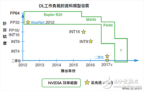
Figure 2 NVIDIA down precision support
However, according to the machine learning deduction benchmarks introduced by NVIDIA on the Tesla P40, GoogLeNet v1 Inference, the efficiency of the INT8 solution is only three times higher than that of the FP32 solution. This result shows that the precision is reduced in the GPU architecture and the efficiency is higher. Difficulty [16].
With machine learning and other workloads shifting to lower accuracy and customization accuracy, GPU vendors need to introduce more new products in the market, and existing users of the manufacturers also need to upgrade their platforms in order to benefit from the development in this area.
Multiple levels of memory to ensure that software-defined data arrives at the path to hardshipSimilar to the CPU, the data flow in the GPU is also defined by software and depends on the rigorous and complex memory hierarchy of the GPU [17]. The typical GPU memory hierarchy is shown in Figure 3. Each thread has its own memory space in the cache file to store the thread's local variables. A small number of threads in the same module can communicate through shared memory; and all threads can communicate through global or off-chip memory [18].
As shown in Figure 3, since the data needs to span the entire memory hierarchy from the buffer file to the global memory, the power consumption and delay associated with memory access are increased by 100 times and 80 times respectively [15][17][19] . In addition, memory conflicts are inevitable. At the same time, delays will increase the ALU's idleness, which will reduce the computing power and efficiency.
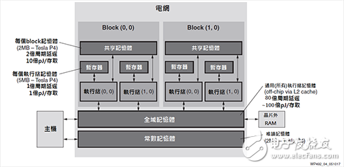
Figure 3 Typical GPU memory hierarchy
Therefore, if you want to exploit the GPU's computing and efficiency potential, the data flow of the workload must be accurately mapped to the GPU memory hierarchy. In fact, few workloads have enough data locality to effectively map to the GPU. For most workloads, when running on a GPU, the actual computing power and efficiency will be greatly reduced, and the solution delay will increase [19][20].
Machine learning inference as a quantitative example can clearly show the limitations of data flow. The GPU must perform 128 batches of batches to achieve a more efficient but longer-delay solution. In the end, batch processing makes machine learning processing local, but at the cost of increased latency [21], and this result can be clearly seen in the NVIDIA P40 benchmark test of GoogLeNet v1 Inference. For GoogLeNet v1, its network is constrained by the computational bandwidth of the P40 memory, so reducing the batch-related memory bandwidth does not help much. However, P40 obviously needs 128 batches to achieve 50% of GPU theoretical performance, but it also increases system latency [16].
In some cases, the data can be pre-processed by the CPU so that the workload can be more efficiently mapped to the GPU SIMT architecture and memory hierarchy, but at the expense of generating more CPU operations and power consumption, thus offsetting the GPU's Advantages [7].
・ Limited I/O optionsAs described in the beginning of this article, the original role of the GPU is as a coprocessor. To facilitate communication with the host, the GPU used to have only one PCIe interface and several external DRAM interfaces such as GDDR5 chips. In recent products, some GPUs use hardware interfaces for GPU-to-GPU communication. The CPU still needs to connect to the network to allocate tasks to the GPU. This not only increases system power consumption, but also causes bottlenecks due to the limited bandwidth of the PCIe. For example, the NVIDIA Tesla 40 supporting PCIe 3.0 & TI;16 can only have 16GB/s of bandwidth.
GPU vendors have begun building small SoCs such as the NVIDIA Tegra X1, which integrates GPU computing, Arm processors, some GM peripherals, and basic Ethernet networks such as HDMI, MIPI, SIP, and CAN. Since these components have a small amount of computing power, they must rely on additional discrete GPUs to achieve the necessary computing power. However, the separation of GPU interfaces has significant limitations. For example, the Tegra X1 only supports PCIe 2.0 & TI;4, leading to serious bottlenecks, and the additional SoC's power consumption will further reduce the efficiency of the platform.
・Chip built-in memory resourcesIn addition to the detrimental effects of latency, efficiency, and transfer rate, the bandwidth of off-chip memory is significantly lower than the local/on-chip memory. Therefore, if the workload needs to rely on off-chip memory, not only the bandwidth of off-chip memory will become a bottleneck, but also the computing resources will be idle, thus reducing the computing power and efficiency that the GPU can provide.
Therefore, it is more advantageous to use large-scale, low-latency, high-bandwidth built-in memory on the chip. Taking machine learning inference as an example, GoogLeNet requires a total of 27.2 MB of memory space; assuming that the GPU is not provided by the FP32, this is not an option. Means that off-chip memory is needed [22]. In many cases, high-cost, high-bandwidth memory (HBM) and batch processing are needed to prevent the core from being idle. If you choose to have larger on-chip memory components, you can avoid HBM costs and additional delay and power consumption issues.
・Power consumption rangeGPU vendors typically apply 250-watt power caps when designing boards and GPUs, and rely on effective thermal management to regulate temperature. For the machine learning inference market, NVIDIA has developed components such as the Tesla M4 and P4 that meet the 75W power consumption range. Although 75W is far beyond the allowed system-level power and thermal range, the absolute power consumption of the GPU is still one of the factors that hinders the widespread adoption of GPUs.
Functional safetyGPUs originate from the fields of consumer image processing and high-performance computing, and there is no need for functional security. However, as GPU vendors target the ADAS market, functional safety becomes a necessary condition. Therefore, for use in ADAS systems, components need to be redesigned to ensure that the required level of functional safety certification is achieved. This is not only a long-term and involved learning process for GPU vendors, but also new tools and equipment.
Multi-application push driver FPGA/SoC benefits・Original computing power
Unlike GPU advocates, the raw computing power provided by a single FPGA component can achieve 38.3 INT8 TOP/s performance. The NVIDIA Tesla P40 accelerator provides similar 40 INT8 TOP/s primitive computing power when running at the base frequency, but power consumption is more than twice that of the FPGA solution [26].
In addition, the flexibility of FPGA components supports the accuracy of various data types [27]. For example, for binarized neural networks, FPGAs can provide ultra-high binary computing capabilities of 500 TOPs/s (assuming 2.5 LUT/ï¡¿ operation), which is equivalent to 25 times the typical GPU performance. Some precisions are more suitable for DSP resources, others can be run in programmable logic, and some are suitable for using the two together. This flexibility ensures that the operation and efficiency of the components can be reduced with precision and reduced to binary. A large number of studies in the field of machine learning have carried out the research of the best precision from the point of view of calculation, precision and efficiency [28~32]. Regardless of the best point, the workload given can be adjusted accordingly.
Over the years, many FPGA users have used systolic array processing to achieve optimal performance for a variety of workloads, including machine learning inference [33][34].
Interestingly, NVIDIA has increased the available computing power and efficiency for today's deep learning workloads, and has enhanced similar functionality in the form of Tensor Core in the Volta architecture. However, deep learning workloads evolve over time, so the Tensor Core architecture also needs to change, and GPU users also need to wait to purchase new GPU hardware.
・Efficiency and power consumption
At the system level, the computing platform must provide maximum computing power within the specified power and thermal range. To meet this requirement, the computing platform must:
1. Within the allowable power range
2. Maximize computing power within the power budget
The All Programmable family of components allows the user to select the component that best matches the power and thermal range. As shown in Table 1, from the perspective of the original operation, this component can provide an efficient general-purpose computing platform for fixed-precision data types, mainly because the indirect overhead in the FPGA architecture is low. For example, GPUs require more complexity around their computing resources to facilitate software programmable functionality. For the tensor operation of today's deep learning workloads, NVIDIA's Tesla V100 leverages the enhanced Tensor Core to achieve efficiencies that rival those of FPGAs and SoCs. However, deep learning workloads are evolving at a very fast pace, so it is impossible to determine how long the efficiency of NVIDIA Tensor Core can sustain in deep learning workloads.
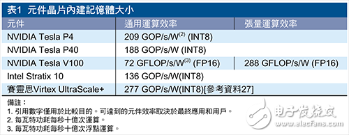
From this perspective, NVIDIA V100 is also facing efficiency challenges for other common workloads. Given the limitations described earlier in this article, it is difficult for GPUs to achieve the numbers shown in Table 1 for actual workloads and systems.
・All Programmable component flexibility
Xilinx combines hardware programmable resources (such as logic, paths, and I/O) with flexible and independent integrated core blocks (such as DSP partitioning and UltraRAM), and builds all of them on leading process technologies, such as TSMC's 16nm FinFET process, and thus achieve this balance.
Hardware programmability and resiliency mean that the underlying hardware is configured to meet the needs of a given workload. Subsequently, the data path can be easily reconfigured through partial reconfigurable functions even during runtime [35]. Figure 4 attempts to illustrate some of the flexibility provided by the All Programmable component. The core (or user design element) can be directly connected to programmable I/O, any other core, LUTRAM, Block RAM and UltraRAM, and external memory.
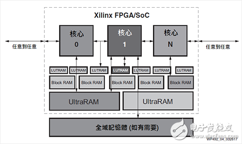
Figure 4 All Programmable data path and various forms of IO
Hardware programmability components mean that they do not have such specific limitations, such as SIMT or fixed data paths. The computing power and efficiency of Xilinx components can be achieved whether it is massive parallelism, moderate parallelism, pipeline continuity, or hybrids. In addition, if the underlying algorithm changes, such as the development of a machine learning network, the platform can also be adjusted accordingly.
In many systems and workloads, the FPGA and SoC components can be seen as having elastic advantages, and machine learning inference is one of them. The trend of machine learning inference is to move towards sparse networks, and FPGA and SoC component users are already taking advantage of this trend, and NVIDIA itself is one of the users. In a recent article written jointly with NVIDIA on speech recognition, it was mentioned that by using an FPGA, the NVIDIA GPU can only increase the speed by 3 times and the efficiency by 11.5 times compared to the CPU, which can increase the speed by 43 times and the efficiency by 40 times.[36] ]. The programmable data path also reduces the batch processing requirements of the FPGA. Batch processing is an important determinant of system latency versus real-time performance.
From a big data perspective, FPGAs are efficient and fast when dealing with complex data, such as variable-length strings, in SQL workloads. Genome analysis is an example. Some people have used GPUs to speed up gene analysis, which is 6 to 10 times faster than Intel Xeon CPUs [40]. However, FPGAs have a higher speed-up effect, which is about 80 times faster than comparable CPUs [41].
Finally, for automotive system designers struggling to develop autonomous driving capabilities, the flexibility of FPGA and SoC components provides them with a scalable platform to meet the SAE's various standards for fully automated driving.
・ Various forms of I/O elasticity
In addition to the flexibility of component computing resources, various forms of FPGA I/O resiliency ensure that components are seamlessly integrated into existing infrastructure, such as directly connecting to a network or storage device without the use of a host CPU.[42] . In addition, I/O resiliency allows the platform to adjust for changes or updates to the infrastructure.
・Chip built-in memory
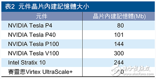
As shown in Table 2, this huge on-chip memory cache represents the majority of workload memory requirements are provided by on-chip memory to reduce memory bottlenecks caused by external memory accesses, as well as HBM2. This type of high-bandwidth memory consumes power and costs. For example, coefficient/enthalt characteristics maps for most deep learning network technologies (eg, GoogLeNet) may exist in the on-chip memory to improve the operation efficiency and reduce the cost. Built-in access to the chip can eliminate the huge delay caused by off-chip memory access and maximize system performance.
・In-package HBM
For applications that require high-bandwidth memory, FPGA components provide HBM to efficiently map workloads to components and available memory bandwidth, maximizing performance and computing efficiency.
In the new era of computing, system designers face many difficult choices. FPGAs and SoCs provide system designers with the lowest risk to assist them in meeting the core requirements and challenges of future systems while providing sufficient flexibility to ensure that the platform will not fall behind in the future. This is a dual requirement. In the deep learning domain, the inherent parallelism of the DSP architecture in the UltraScale architecture, through the spreadability of the dot product of the INT8 vector, enhances the convolutional and matrix multiplication rates for neural networks, allowing deep learning inferences to reach lower latency. The combination of fast DSP arrays, the most efficient Block RAM memory hierarchy, and the UltraRAM memory array provides the best power efficiency.
Plano-concave lenses diverge the light, with a negative focal length, one of which is flat and the other is concave. It is often used for beam expansion, projection and enlargement of the focal length of the optical system. Antireflection coating options include UV, VIS, NIR, and SWIR.
Plano-concave lenses with negative focal length are often used in imaging or beam collimation applications. Coated lenses are also widely used in visible light and near-infrared fields. Germanium, silicon or zinc selenide substrates are suitable for infrared applications, and fused silica is suitable for ultraviolet application.
Plano Concave Lens,Quartz Plano Concave Lens,Concave Lenses,N-Bk7 Plano Concave Lens Lens
Bohr Optics Co.,Ltd , https://www.bohr-optics.com