Abstract: This application note explains how to connect the DS1390 to a Motorola DSP with a built-in SPI â„¢ interface. This circuit uses the Motorola DSP56F800DEMO development board and CodeWarrior IDE.
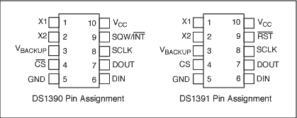
The DS1390 real-time clock (RTC) can be connected to a microcontroller (µC) or digital signal processor (DSP) unit through an SPI interface. This application note shows how to connect the DS1390 to a Motorola DSP with a built-in SPI interface. This circuit uses the Motorola DSP56F800DEMO development board and CodeWarrior® IDE. Using the routine This routine starts with a new blank project. For details, please refer to the Motorola Toolkit Installation Guide Guide: Creating a CodeWarrior Project. The additional code for this application note is in main.c. Operation process The program controls the CS of the DS1390 through the GPIO port. The SPI controller is initialized by software, and the DSP writes the time and date to the DS1390. The software can then read the time and date cyclically. DS1390 and DS1391 support SPI Mode 1 and Mode 3.
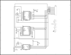
The schematic diagram is shown in Figure 1. The circuit contains a daughter card with a Motorola development board. Please note that the circuit in Figure 1 includes several RTCs with an SPI interface. Only one RTC is required at a time. This article shows that the program only supports DS1390. The program list is shown in Figure 2.

figure 1.

Detailed circuit diagram (PDF, 138kB)
Figure 2. Schematic of daughter card
Figure 3. Program list
/ * File: DS1390.c * / / * This example program was developed using the Motorola 56F800 Demo Board Kit. Follow the kit instalaTIon guide for creaTIng a CodeWarrior Project. Use the shell of the new project for this example. Note: This program is for example only and is not supported by Dallas Semiconductor Maxim. * / #include "port.h" #include "stdio.h" #include "stdlib.h" / ************* ****************************************** * Main program for use with Embedded SDK ************************************************** ***** / extern sampleASM (void); void reset_spi (void); void wbyte_spi (unsigned char); void init_sci0 (Word16); tx_sci0 (unsigned char); void bcd2ascii (unsigned char); unsigned char rbyte_spi (void) ; #define REG_BASE 0x0000 #define SCI0_BASE 0x0F00 #define SPI_BASE 0x0F20 #define GPIOA_BASE 0x0FB0 #define GPIOB_BASE 0x0FC0 #define SCI0_SCIBR * (volaTIle UWord16 *) (SCI0_BASE + 0) #define SCI0_SCI (SCI0) (SCI 0) define SCI0_SCISR * (volatile UWord16 *) (SCI0_BA SE + 2) #define SCI0_SCIDR * (volatile UWord16 *) (SCI0_BASE + 3) #define SPSCR * (volatile UWord16 *) (SPI_BASE + 0) #define SPDSR * (volatile UWord16 *) (SPI_BASE + 1) #define SPDRR * (volatile UWord16 *) (SPI_BASE + 2) #define SPDTR * (volatile UWord16 *) (SPI_BASE + 3) #define GPIO_A_PUR * (volatile UWord16 *) (GPIOA_BASE + 0) #define GPIO_A_DR * (volatile UWord16 *) (GPIOA_BASE + 1) #define GPIO_A_DDR * (volatile UWord16 *) (GPIOA_BASE + 2) #define GPIO_A_PER * (volatile UWord16 *) (GPIOA_BASE + 3) #define GPIO_B_PUR * (volatile UWord16 *) (GPIOB_BASE + 0) #define GPIO_B_DR * (volatile UWord16 *) (GPIOB_BASE + 1) #define GPIO_B_DDR * (volatile UWord16 *) (GPIOB_BASE + 2) #define GPIO_B_PER * (volatile UWord16 *) (GPIOB_BASE + 3) void main (void) (unsigned char msec = 0, min = 0x26, sec = 0x00, hr = 0x17, dow = 0x06, date = 0x26, mon = 0x12, yr = 0x03, write = 0; reset_spi (); init_sci0 (195); // 30MHz / 195 = 9600 baud GPIO_B_DR = 0x0008 ; // disable RTC-CS high GPIO_B_DR = 0; // enable RTC-CS low wbyte_spi (0x8d); // co ntrol register write address rbyte_spi (); // dummy read wbyte_spi (0x18); // enable osc, 32kHz sqw rbyte_spi (); GPIO_B_DR = 0x0008; // disable RTC-CS high if (write) {GPIO_B_DR = 0; // enable RTC-CS low wbyte_spi (0x80); // select seconds register write address rbyte_spi (); // dummy read wbyte_spi (msec); // milliseconds register data rbyte_spi (); wbyte_spi (sec); // seconds register data rbyte_spi (); wbyte_spi (min); // minutes register rbyte_spi (); wbyte_spi (hr); // hours register rbyte_spi (); wbyte_spi (dow); // day of week register rbyte_spi (); wbyte_spi (date); / / date register rbyte_spi (); wbyte_spi (mon); // month register rbyte_spi (); wbyte_spi (yr); // year register rbyte_spi (); GPIO_B_DR = 0x0008; // disable RTC-CS high} while (1) { GPIO_B_DR = 0u; // enable RTC-CS low wbyte_spi (0); // seconds register read address rbyte_spi (); // dummy read wbyte_spi (0); msec = rbyte_spi (); // read milliseconds register wbyte_spi (0) ; sec = rbyte_spi (); // read seconds register wbyte_spi (0); m in = rbyte_spi (); // ditto minutes wbyte_spi (0); hr = rbyte_spi (); // and so on wbyte_spi (0); dow = rbyte_spi (); wbyte_spi (0); date = rbyte_spi (); wbyte_spi ( 0); mon = rbyte_spi (); wbyte_spi (0); yr = rbyte_spi (); GPIO_B_DR = 0x0008; // disable RTC-CS high tx_sci0 (0x0d); // sequence to print time & date tx_sci0 (0x0a); bcd2ascii (yr); tx_sci0 ('/'); bcd2ascii (mon); tx_sci0 ('/'); bcd2ascii (date); tx_sci0 (''); bcd2ascii (hr); tx_sci0 (':'); bcd2ascii (min) ; tx_sci0 (':'); bcd2ascii (sec);} return;} // SPSCR // 15 14 13 12 11 10 9 8 7 6 5 4 3 2 1 0 // r MSB SPRF ERRIE ovrf modf spte modfen spr1 spr0 sprie spmstr cpol cpha spe spite void reset_spi () {int val; SPSCR = 0x0056; // SPR0, SPMSTR, CPHA, SPE SPDSR = 0x0007; // 8-bit size SPSCR & = 0xfffd; // clear spe, resets SPI ( partial) SPSCR | = 0x0002; // set spe, new values ​​take effect GPIO_B_PER = 0x00f3; // use GPIOB3 as CS for RTC GPIO_B_DDR = 0x000d; // direction is output GPIO_A_PER = 0x00f9; // enable / disable per function (1 = enable) GPIO_A_DD R = 0x0006; // direction is output (1 = output) GPIO_A_DR = 0; // write bits low (0 = low)} void wbyte_spi (unsigned char wbyte) // ------ write one byte --- ---- {while (! (SPSCR & 0x0200)); // wait for transmitter empty flag SPDTR = wbyte;} void bcd2ascii (unsigned char dat) // ----- convert bcd to ascii and send to sci- --- {tx_sci0 ((dat >> 4) + 0x30); tx_sci0 ((dat & 0x0f) + 0x30);} unsigned char rbyte_spi (void) // -------- read one byte --- ------- {while (! (SPSCR & 0x2000)); // wait for receiver full flag return (SPDRR);} void init_sci0 (Word16 baud) {GPIO_B_PER = 0x00f3; // set up GPIO_B_DDR = 0x000d; // direction is output SCI0_SCIBR = baud; // baud rate SCI0_SCICR = 0x2000; // control reg} tx_sci0 (unsigned char val) {UWord16 reg; SCI0_SCICR & = 0xfffb; // turn receiver off SCI0_SCICR | = 8; // turn transmitter on do {reg = SCI0_SCISR; // clear flag by reading} while ((reg & 0x8000) == 0); // wait until RDRF is false SCI0_SCIDR = (unsigned int) (val);}
Navigator Speaker
Navigator speaker:
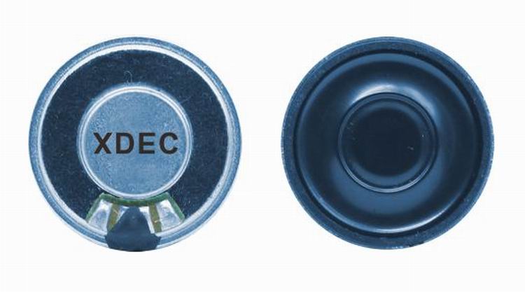
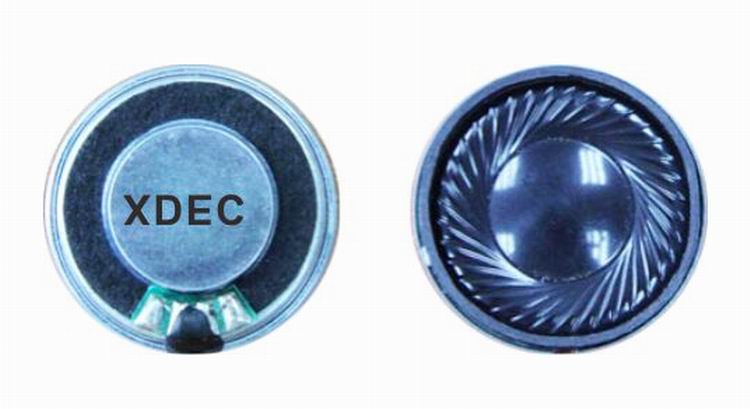
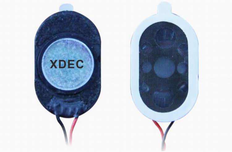
Navigator speaker is a kind of micro speaker unit which uses a diaphragm made of Mylar material. Mylar speakers are of ultrathin design and lightweight and clear voice. It is widely used in car electronics (GPS navigator, digital video recorder, radar detector-).
There are two types of Mylar speakers from the shapes:
1) Round shapes, we have products from 10mm to 57mm in diameter.
2) Oblong shape, we have products in sizes of 1510/1712/1813-..


FAQ
Q1. What is the MOQ?
XDEC: 2000pcs for one model.
Q2. What is the delivery lead time?
XDEC: 15 days for normal orders, 10 days for urgent orders.
Q3. What are the payment methods?
XDEC: T/T, PayPal, Western Union, Money Gram.
Q4. Can you offer samples for testing?
XDEC: Yes, we offer free samples.
Q5. How soon can you send samples?
XDEC: We can send samples in 3-5 days.
Navigator Speaker,Gps Speaker,Radar Speaker,Vehicle Navigation Speakers
Shenzhen Xuanda Electronics Co., Ltd. , https://www.xdecspeaker.com
