The buzzer is divided into a piezoelectric buzzer and an electromagnetic buzzer from the structure. The piezoelectric type is the piezoelectric ceramic sheet, and the current is relatively small. The electromagnetic buzzer is used to energize and vibrate the coil, and the volume is relatively small.
According to the driving method, it is divided into active buzzer and passive buzzer. Active and passive here do not refer to the power source, but to the source of the oscillation. The active buzzer has an internal oscillation source. As shown in Figure 9-8, the BUZZ pin is given a low level and the buzzer will sound directly. The passive buzzer does not have an internal oscillation source. It must be given a pulse frequency signal between 500 Hz and 4.5 kHz to drive it. Active buzzer is often more expensive than passive buzzer, because there are more oscillating circuits inside, the driving pronunciation is simple, it can be driven by level, and the passive buzzer is cheaper, in addition to passive buzzer The sound frequency can be controlled, and the scale and frequency have a certain correspondence, so you can make the effect of “do re mi fa sol la siâ€, you can use it to make simple music tracks, such as birthday songs, two tigers. and many more.
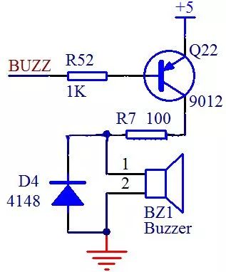
Figure 9-8 Schematic diagram of the buzzer circuit
Let's take a look at the circuit in Figure 9-8. The buzzer current is still relatively large, so it needs to be driven by a triode and a 100 ohm resistor is added as a current limiting resistor. In addition, a D4 diode is added. This diode is called a freewheeling diode. Our buzzer is an inductive device. When the triode is turned on to power the buzzer, an on current flows through the buzzer. And we know that one characteristic of the inductor is that the current cannot be abruptly changed, and the current is gradually increased when it is turned on. This is no problem, but when it is turned off, the circuit of "power-triode-buzzer-ground" is passed. Truncate, can't pass any current, then where is the stored current going through the D4 and the buzzer's own loop, thus avoiding the reverse shock caused by the inductor current during turn-off? . The current when the switch is turned off, this is the origin of the name of the freewheeling diode.
Buzzers are often used for making sounds on computers, printers, and multimeters. The sound is usually very simple. It is simple to make a sound. We simply use the program to make a sound at 4KHZ and a sound at 1KHZ. Programs, students can study the program themselves and compare the actual results.
#include
Sbit BUZZ = P1^6; // buzzer control pin
Unsigned char T0RH = 0; //High byte of the T0 overload value
Unsigned char T0RL = 0; //low byte of the T0 overload value
Void OpenBuzz(unsigned int frequ);
Void StopBuzz();
Void main(){
Unsigned int i;
TMOD = 0x01; //Configure T0 to work in mode 1, but not start first
EA = 1;
While (1){ //Enable global interrupt
OpenBuzz(4000); //Start the buzzer at 4KHz
For (i=0; i> 8); //16-bit overload value is decomposed into high and low two bytes
T0RL = (unsigned char) reload;
TH0 = 0xFF; //Set an initial value close to overflow to make the timer work immediately
TL0 = 0xFE;
ET0 = 1; //Enable T0 interrupt
TR0 = 1; //Start T0
}
/* Buzzer stop function */
Void StopBuzz(){
ET0 = 0; // disable T0 interrupt
TR0 = 0; //stop T0
}
/* T0 interrupt service function for controlling buzzer sound*/
Void InterruptTimer0() interrupt 1{
TH0 = T0RH; //Reload the reload value
TL0 = T0RL;
BUZZ = ~BUZZ; //Reverse buzzer control level
} Another buzzer is used to output music. It is just fun. There are very few applications. The content of the scales and music scores is included inside. The program is also a bit complicated, so it will not be explained in detail. Only one program that can play "Two Tigers" can be downloaded and played on the board to satisfy curiosity.
#include
Sbit BUZZ = P1^6; // buzzer control pin
Unsigned int code NoteFrequ[] = { //Intermediate 1-7 and treble 1-7 corresponding frequency list
523, 587, 659, 698, 784, 880, 988, //Middle 1-7
1047, 1175, 1319, 1397, 1568, 1760, 1976 // treble 1-7
};
Unsigned int code NoteReload[] = { //The timer reload value corresponding to midrange 1-7 and treble 1-7
65536 - (11059200/12) / (523*2), //Middle 1
65536 - (11059200/12) / (587*2), //2
65536 - (11059200/12) / (659*2), //3
65536 - (11059200/12) / (698*2), //4
65536 - (11059200/12) / (784*2), //5
65536 - (11059200/12) / (880*2), //6
65536 - (11059200/12) / (988*2), //7
65536 - (11059200/12) / (1047*2), //High pitch 1
65536 - (11059200/12) / (1175*2), //2
65536 - (11059200/12) / (1319*2), //3
65536 - (11059200/12) / (1397*2), //4
65536 - (11059200/12) / (1568*2), //5
65536 - (11059200/12) / (1760*2), //6
65536 - (11059200/12) / (1976*2), //7
};
Bit enable = 1; //buzzer sound enable flag
Bit tmrflag = 0; //Timer interrupt completion flag
Unsigned char T0RH = 0xFF; //T0 high byte of the reload value
Unsigned char T0RL = 0x00; //low byte of the T0 overload value
Void PlayTwoTiger();
Void main(){
Unsigned int i;
EA = 1; //Enable global interrupt
TMOD = 0x01; //Configure T0 to work in mode 1
TH0 = T0RH;
TL0 = T0RL;
ET0 = 1; //Enable T0 interrupt
TR0 = 1; //Start T0
While (1){
PlayTwoTiger(); //Play music--two tigers
For (i=0; i> 8;
T0RL = NoteReload[note];
/ / Calculate the total time of the beat, shifting 2 bits to the right is equivalent to 4, shifting instead of division can speed up execution
beatTime = (TwoTigerBeat[beat] * NoteFrequ[note]) >> 2;
/ / Calculate the sounding time, which is 0.75 of the total time. The shift principle is the same as above.
soundTime = beatTime - (beatTime >> 2);
Enable = 1; //Instruct the buzzer to start sounding
Time++;
}else{ //Process the current beat if the current beat is not finished
//The current duration reaches zero when the total time of the beat is reached.
//and increment the beat index to prepare to start a new beat
If (time >= beatTime){
Time = 0;
Beat++;
}else{ //When the current duration does not reach the total time,
Time++; // accumulate time count
//After reaching the utterance time, the indicator turns off the buzzer.
/ / Insert a silence interval of 0.25 * total time,
If (time == soundTime){
Enable = 0; / / to distinguish between two consecutive beats
}
}
}
}
}
/* T0 interrupt service function for controlling buzzer sound*/
Void InterruptTimer0() interrupt 1{
TH0 = T0RH; //Reload the reload value
TL0 = T0RL;
Tmrflag = 1;
If (enable){ //Invert the buzzer control level when enabled
BUZZ = ~BUZZ;
}else{ // Turn off the buzzer when not enabled
BUZZ = 1;
}
}
6 Layer PCB
6 Layer PCB - stackup & prototype & price & manufacturing
What is 6 Layer PCB?
6 layer PCB board is, in general, a 4 Layer PCB board with 2 extra signal layers added between the planes. The 6-layer PCB classic stackup includes 4 routing layers (2 outer layers + 2 internal layers) and 2 internal planes (one for ground and the other for power). This enhances the EMI dramatically by offering 2 buried layers for high-speed signals and 2 surface layers for routing low-speed signals. The signal layers should be closed to the adjacent planes.
6 Layer PCB Prototype Fabrication China Manufacturer
Jinghongyi PCB has been committed to the production of multi-layer PCB and prototype PCB for nearly 10 years. The largest number of multi-layer printed circuit boards for customers are 4-layer, 6-layer, 8-layer, 10 layer, 12 Layer PCB and above. In order to ensure the quality of PCB products, we constantly improve and upgrade the production process. PCB surface treatment technology has hot air leveling(HASL), OSP, electroless nickel, immersion gold, immersion silver, immersion tin and so on.
The printed circuit board is basically composed of the pad, via, solder mask layer, silkscreen layer, copper wire, and other parts. Among them, solder mask refers to the part covered by ink on PCB. Because most PCB uses green ink, the green ink part that can be seen is solder mask. The role of the solder mask in controlling the reflow welding process is very important. In addition to green ink, the welding layer can According to the different needs of customers, and can also be customized in a variety of colors, such as green, blue, black, red, white, yellow, purple. Of course, the price will vary with the color of the solder mask. Green oil is the one with low price and stable quality, which is also the reason why green oil is most used. The price of black oil, red oil, and white oil is almost the same, slightly more expensive than green oil, and the price of rare inks such as yellow and violet oil is the highest. In addition to the color of the solder resist ink, there are also matte and bright, matte ink color.
Based on our very experienced PCB engineer, we can help you in the 6-layer PCB stack up and design as much as possible.
In addition to providing you with 6-layer PCB and prototype manufacturing, we also provide one-stop prototype assembly services, including electronic components procurement, stencil, etc. The turnkey printed circuit board assembly services make your R&D work easy and time-saving.
6 Layer PCB Stackup and Design
What is PCB stack UP?
PCB Stack up refers to the arrangement of copper and insulation layers that make up PCB before the layout design of circuit board. Although stacking allows you to get more circuits on a single board through various PCB layers, the structure of PCB stacking design has many other advantages:- The PCB layer stack can help you minimize circuit noise and radiation and reduce impedance and crosstalk problems in high-speed PCB layouts.
- A good stacked PCB stack can also help you balance the need for low-cost, efficient manufacturing methods and focus on signal integrity issues.
- Proper PCB stacking can enhance the electromagnetic compatibility of your design.
- For PCB-based applications, stacked PCB configurations are usually good for you.
Why do PCBs stack up?
The irreversible development of modern electronic products has increasingly pushed PCB towards such needs as miniaturization, light weight, high speed, better functionality and reliability, and longer life, which has led to the popularity of multi-layer PCB. Two or more Single Sided PCB and/or Double Sided PCB are stacked together by a combination of semi-solid adhesives called "prepregs" to form multilayer PCBs through reliable predefined interconnections between them. There are three or more conductive layers in a Multilayer PCB, two of which are outside, and one is synthesized in an insulating board. With the increasing complexity and density of PCB, some problems may arise, such as noise.
One of the most important factors to determine the performance of product electromagnetic compatibility (EMC) is to plan the optimal multi-layer stack up. The carefully designed cascade can minimize radiation and prevent the circuit from being disturbed by external noise sources. Good stacked PCB substrates can also reduce signal crosstalk and impedance mismatch. However, poorer stacking may increase EMI radiation, because impedance mismatch will lead to reflection and ringing in the system, which will greatly reduce the performance and reliability of the product. Then, this article will focus on the layer stack definition, design rules and basic considerations.
Most six-layer PCB consist of four signal routing layers and two planes. From an EMC perspective, a 6-layer Printed circuit board is usually better than a 4 layer PCB board.
6 Layer PCB Stackup
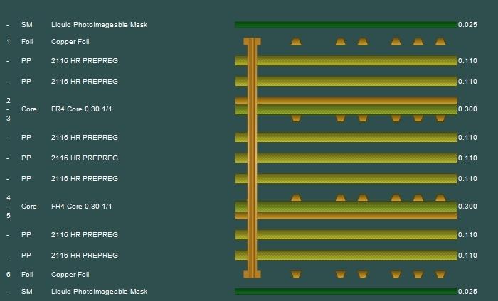
6 layer 1.6 MM standard stackup and thickness
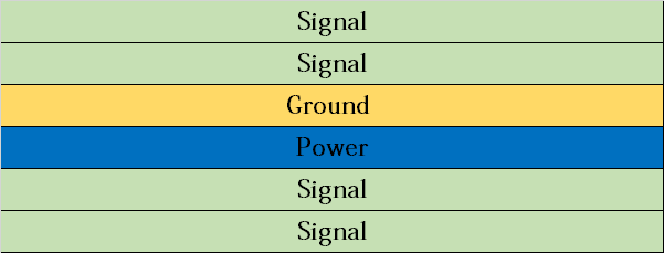
Fig. 1 One of the stackup methods of 6-layer PCB
With six layers available the principle of providing two buried layers for high-speed signals is easily implemented as shown in Fig. 2. This configuration also provides two surface layers for routing low speed signals.

Fig. 2 Less common 6 layer PCB stackup
Not nearly as common, but a good performing stack-up for a six-layer PCB is shown in Fig. 2.
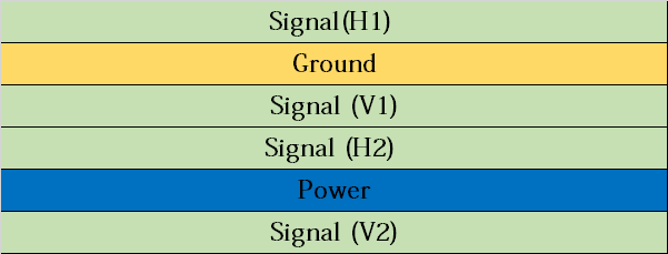
Fig. 3 Another performing six-layer PCB board stackup
Another excellent performing six-layer PCB board stackup is shown in Fig. 4. It provides two buried signal layers and adjacent power and ground planes and satisfies all five objectives. The big disadvantage, however, is that it only has two routing layers -- so it is not often used.
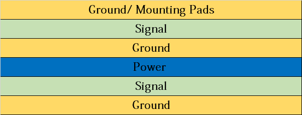
Fig. 4 Another excellent performing six-layer PCB board stackup
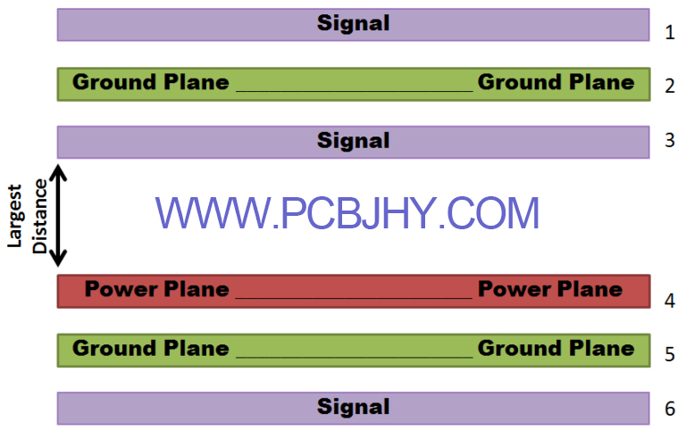
6 Layer PCB Stackup for EMI/EMC
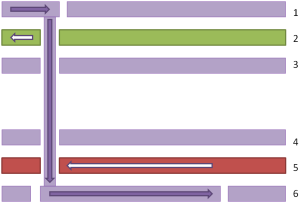
EMI/EMC Return Current 6 Layer PCB Issue
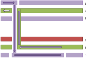
EMI/EMC Return Current 6 Layer PCB Solved
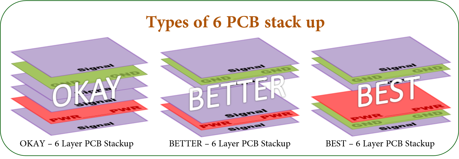
Types of 6 PCB stack up-how to choose?
PCB materials and stackup thickness commonly used in multilayer circuit boards.
| 6 Layer Stackup - 0.8mm thickness | ||||||
| layer order | layer name | material type | material description | dielectric constant | thickness | copper weight |
| 1 | top | copper | signal | 0.035mm | 1 oz | |
| 2116 | prepreg | 4.5 | 0.12mm | |||
| 2 | inner 1 | copper | plane | 1 oz | ||
| core | 4.6 | 0.2mm | ||||
| 3 | inner 2 | copper | plane | 1 oz | ||
| 2116 | prepreg | 4.5 | 0.12mm | |||
| 4 | inner 3 | copper | plane | 1 oz | ||
| core | 4.6 | 0.2mm | ||||
| 5 | inner 4 | copper | plane | 1 oz | ||
| 2116 | prepreg | 4.2 | 0.12mm | |||
| 6 | bottom | copper | signal | 0.035mm | 1 oz | |
| Final board thickness: 0.8mm±0.1mm | ||||||
| 6 Layer Stackup - 1.0mm thickness | ||||||
| layer order | layer name | material type | material description | dielectric constant | thickness | copper weight |
| 1 | top | copper | signal | 0.035mm | 1 oz | |
| 2116 | prepreg | 4.5 | 0.12mm | |||
| 2 | inner 1 | copper | plane | 1 oz | ||
| core | 4.6 | 0.3mm | ||||
| 3 | inner 2 | copper | plane | 1 oz | ||
| 2116 | prepreg | 4.5 | 0.12mm | |||
| 4 | inner 3 | copper | plane | 1 oz | ||
| core | 4.6 | 0.3mm | ||||
| 5 | inner 4 | copper | plane | 1 oz | ||
| 2116 | prepreg | 4.2 | 0.12mm | |||
| 6 | bottom | copper | signal | 0.035mm | 1 oz | |
| Final board thickness: 1.0mm±0.1mm | ||||||
| 6 Layer Stackup - 1.6mm thickness (preferred materials) | ||||||
| layer order | layer name | material type | material description | dielectric constant | thickness | copper weight |
| 1 | top | copper | signal | 0.035mm | 1 oz | |
| 2116 | prepreg | 4.5 | 0.12mm | |||
| 2 | inner 1 | copper | plane | 1 oz | ||
| core | 4.6 | 0.6mm | ||||
| 3 | inner 2 | copper | plane | 1 oz | ||
| 2116 | prepreg | 4.5 | 0.12mm | |||
| 4 | inner 3 | copper | plane | 1 oz | ||
| core | 4.6 | 0.6mm | ||||
| 5 | inner 4 | copper | plane | 1 oz | ||
| 2116 | prepreg | 4.2 | 0.12mm | |||
| 6 | bottom | copper | signal | 0.035mm | 1 oz | |
| Final board thickness: 1.6mm±0.1mm | ||||||
| 6 Layer Stackup - 1.6mm thickness (non-preferred materials but possible) | ||||||
| layer order | layer name | material type | material description | dielectric constant | thickness | copper weight |
| 1 | top | copper | signal | 0.035mm | 1 oz | |
| 2116 | prepreg | 4.7 | 0.2mm | |||
| 2 | inner 1 | copper | plane | 1 oz | ||
| core | 4.6 | 0.5mm | ||||
| 3 | inner 2 | copper | plane | 1 oz | ||
| 2116 | prepreg | 4.5 | 0.12mm | |||
| 4 | inner 3 | copper | plane | 1 oz | ||
| core | 4.6 | 0.6mm | ||||
| 5 | inner 4 | copper | plane | 1 oz | ||
| 2116 | prepreg | 4.7 | 0.2mm | |||
| 6 | bottom | copper | signal | 0.035mm | 1 oz | |
| Final board thickness: 1.6mm±0.1mm | ||||||
| 6 Layer Stackup - 2.0mm thickness (preferred materials) | ||||||
| layer order | layer name | material type | material description | dielectric constant | thickness | copper weight |
| 1 | top | copper | signal | 0.035mm | 1 oz | |
| 7630 | prepreg | 4.7 | 0.2mm | |||
| 2 | inner 1 | copper | plane | 1 oz | ||
| core | 4.6 | 0.6mm | ||||
| 3 | inner 2 | copper | plane | 1 oz | ||
| 7630 | prepreg | 4.7 | 0.2mm | |||
| 4 | inner 3 | copper | plane | 1 oz | ||
| core | 4.6 | 0.6mm | ||||
| 5 | inner 4 | copper | plane | 1 oz | ||
| 7630 | prepreg | 4.7 | 0.2mm | |||
| 6 | bottom | copper | signal | 0.035mm | 1 oz | |
| Final board thickness: 2.0mm±0.2mm | ||||||
6
Layer Stackup - 2.0mm thickness (non-preferred materials but possible)
layer order
layer name
material type
material description
dielectric constant
thickness
copper weight
1
top
copper
signal
0.035mm
1 oz
2116+7628
prepreg
4.7+4.7
0.12mm+0.185mm
2
inner 1
copper
plane
1 oz
core
4.6
0.6mm
3
inner 2
copper
plane
1 oz
2116
prepreg
4.7
0.12mm
4
inner 3
copper
plane
1 oz
core
4.6
0.6mm
5
inner 4
copper
plane
1 oz
2116+7628
prepreg
4.7+4.7
0.12mm+0.185mm
6
bottom
copper
signal
0.035mm
1 oz
Final board
thickness: 2.0mm±0.2mm
6 Layer PCB Quote and Price
6 Layer PCB Prototype Price
Of course, at the same time, we also provide sample production services for other PCB products to verify your design as soon as possible.
With regard to delivery, we can provide 24-hour, 72-hour urgent service. No matter where you are in the world.
6 Layer PCB Manufacturing
- Manufacturable PCB Layers
We have abundant experience in manufacturing multi-layer circuit boards, not only in the production process, but also have many years of professional PCB engineers.So if you have multilayer PCB to produce, no matter how many layers, just let us know.
- What size of 6-layer circuit boards can you produce?
According to our PCB manufacturing capability, we have no size limitation.
- PCB Laminate Types
We offer a variety of PCB laminates ranging from FR4 130Tg for lower heating temperatures up to FR4 180Tg for higher temperatures. Also offered are Polyimide, Taconic, Rogers and Nelco material types.
- Manufacturable Thickness of 6-Layer Circuit Board
As with the number of PCB layers we can manufacture, we still have no restrictions on the thickness of the six-layer PCB and can manufacture it.
- PCB Surface Finish Types
We offer various PCB finishes including HASL (Solder), ENIG, Immersion Silver, Immersion Tin, Hard Gold, Entek/OSP, Unclad, Pb Free HASL, Selective Gold and ENEPIG.
Why order 6 layer PCB from JHY PCB?
You will get it after check below advantages.
1. Good quality and price: We are experienced in producing six layer PCB, cost and time can be controlled well. This can help our customer to order good boards in cost-effective price.
2. Short Turnaround Times:
3. No Minimum Quantity: 1 pcs of PCB can be offered.
4. More orders, more discount.
5. Custom PCB Sizes
Printed Circuit Boards,6 Layer PCB,6 Layer PCB Price,6 Layer PCB Prototype
JingHongYi PCB (HK) Co., Limited , https://www.pcbjhy.com